Back to the on-screen lesson ·
Bands from the orbitals of a crystal, conductors, semiconductors and insulators, band gaps and the light they absorb and emit, and n-type and p-type doping.
Paper packet. Every task here also exists on screen, where it is checked automatically; answers written on paper are not assessed by Nydus. When you are back at a device, enter your answers there.
By the end of this lesson you will be able to classify a solid by its band gap, convert a gap to the wavelength it absorbs or emits, and predict how a dopant changes a semiconductor.
Lesson 24 combined two atomic orbitals into one bonding and one antibonding molecular orbital. Lesson 14 turned the wavelength of absorbed light into an energy gap. And from general chemistry you know that metals conduct electricity and most other solids do not. This lesson extends the molecular orbital picture from two atoms to a whole crystal, and uses it to explain conductors, semiconductors and insulators.
| Term | What it means |
|---|---|
| Band | A near-continuous range of energy levels formed when the orbitals of very many atoms combine. |
| Valence band | The highest band filled with electrons, which in a semiconductor holds the bonding electrons. |
| Conduction band | The empty band above the valence band, where electrons can move freely. |
| Band gap, $E_g$ | The energy separating the top of the valence band from the bottom of the conduction band. |
| Semiconductor | A solid with a band gap small enough that some electrons cross it, often between about 0.5 and 3.5 eV. |
| Hole | An empty place in the valence band that behaves as a moving positive charge. |
| Doping | Adding a trace of an impurity to control a semiconductor's carriers. |
| Electron volt, eV | The energy an electron gains across one volt; $1$ eV per particle is $96.485$ kJ/mol. |
Two atoms combine one orbital each into one bonding and one antibonding molecular orbital. Three atoms give three orbitals, spread over a wider range of energy; four give four. A crystal of $N$ atoms gives $N$ orbitals, and with $N$ near $10^{23}$ they lie so close together that they form a continuous band of energy. A crystal of sodium has a band built from its 3s orbitals, a crystal of silicon bands built from its bonding and antibonding combinations of 3s and 3p.
What matters for conduction is how full the bands are. An electron can carry current only if it can move into a slightly higher empty level; in a completely filled band there is nowhere to move. So:
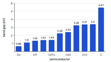
The chart sets the gaps of common semiconductors side by side. A photon can lift an electron across the gap only if its energy is at least $E_g$. With energy in electron volts and wavelength in nanometers, $E = hc/\lambda$ becomes
$$E_g\,(\text{eV}) = \frac{1240}{\lambda\,(\text{nm})}.$$
So silicon absorbs all light shorter than $1240/1.12 \approx 1107$ nm, the whole visible range and some infrared, which is why a silicon wafer looks dark and why silicon makes good solar cells. Gallium nitride, with a gap of $3.40$ eV, absorbs only below $365$ nm and so is transparent to visible light. Run the process in reverse, and an electron falling across the gap emits a photon of that energy: the principle of the light-emitting diode.
Another way: picture
Picture a parking garage with two levels. The lower level, the valence band, is completely full, so no car can move. The upper level, the conduction band, is empty and wide open. In a metal the lower level has empty spaces, so cars move freely. In a semiconductor a short ramp joins the levels, and a few cars get up it, moving freely upstairs and leaving spaces behind them downstairs that other cars can shuffle into. In an insulator the ramp is too steep to climb.
Another way: steps
When an electron in a semiconductor is lifted into the conduction band, it leaves an empty place behind in the valence band. That empty place is a hole. A neighboring electron can move into it, leaving a new hole where it came from, so the hole moves through the crystal, and because it is the absence of a negative charge it behaves as a moving positive charge. A pure semiconductor conducts by equal numbers of electrons and holes.
Heat lifts electrons across the gap, and the number that make it grows very fast with temperature. That is the opposite of a metal, whose conductivity falls as it warms because its vibrating atoms scatter the moving electrons. A semiconductor's conductivity rises with temperature, and a thermistor, the small device in a digital thermometer, uses exactly that rise to measure how warm something is.
Pure silicon conducts poorly at room temperature, because few electrons cross a gap of $1.12$ eV. Doping changes that by adding an impurity at a level of a few parts per million. Each silicon atom uses its four valence electrons in four bonds to its neighbors.
Replace one silicon atom with phosphorus, from group 15, with five valence electrons. Four go into bonds; the fifth is barely held and is easily freed into the conduction band. The dopant donates electrons, and the silicon becomes n-type, conducting by negative carriers. Replace a silicon atom with boron, from group 13, with three. One bond is an electron short, a hole that a neighboring electron can move into. The dopant accepts electrons, and the silicon becomes p-type, conducting by positive holes. A dopant from the same group, such as germanium, bonds just as silicon does and adds no carriers.
Joining n-type and p-type silicon makes a p-n junction, the heart of diodes, transistors, solar cells and light-emitting diodes. At the junction, electrons from the n side meet holes from the p side, and the way they combine or separate is what these devices exploit.
Because the gap sets the color of light a device emits or absorbs, much of semiconductor chemistry is the art of choosing the gap. It depends on the atoms and the bonding. Down a group, the gap shrinks as the atoms get larger and their orbitals overlap more loosely: diamond $5.47$, silicon $1.12$, germanium $0.66$ eV. Across a row, compounds of elements from either side of group 14 have larger gaps than the group 14 element between them, because their bonds are partly ionic: gallium arsenide has $1.42$ eV, more than germanium, its neighbor.
Mixing compounds tunes the gap continuously. Indium gallium nitride, a mixture of indium nitride and gallium nitride, has a gap that can be set anywhere from about $0.7$ to $3.4$ eV by changing the proportion of indium, and blue and green LEDs are made from it. Gallium arsenide phosphide covers the red to yellow range the same way.
Three checks catch most slips. First, the direction: a larger gap means a shorter wavelength. If a material with a wide gap comes out absorbing at a long wavelength, the division has been inverted. Second, the constant: $1240$ converts electron volts and nanometers into each other, and $96.485$ converts electron volts per particle into kilojoules per mole. Multiplying the gap by $1240$ instead of dividing gives a wavelength of thousands of nanometers for a blue emitter, which is plainly wrong.
Third, the classification. Common semiconductors have gaps from a few tenths of an electron volt to about three and a half; a gap of zero means a metal and one above five or so an insulator. For doping, count valence electrons, not atomic numbers: what matters is whether the dopant brings one more or one fewer electron than the atom it replaces.
Red and green LEDs were available by the 1960s and 1970s, but a bright blue one needed a semiconductor with a gap near $2.7$ to $3.4$ eV that could be grown as good crystals and doped both n-type and p-type. Gallium nitride had the right gap, but for decades no one could make p-type gallium nitride.
Isamu Akasaki, Hiroshi Amano and Shuji Nakamura solved the problem in the late 1980s and early 1990s, making efficient blue LEDs from gallium nitride and indium gallium nitride, and shared the 2014 Nobel Prize in Physics for it. Blue light made white LED lighting possible: a blue LED coated with a yellow-emitting phosphor gives white light. White LEDs use a small fraction of the electricity of incandescent bulbs, and the U.S. Department of Energy projects large national energy savings as homes and businesses switch to them.
A solar cell turns light into electricity by lifting electrons across its gap, and the gap decides how much of the sunlight it can use. Photons with less energy than the gap pass straight through and are wasted; photons with more energy are absorbed, but the excess above the gap is lost as heat. A gap near $1.1$ to $1.4$ eV balances the two losses best for sunlight, which is why silicon, at $1.12$ eV, and cadmium telluride, at $1.44$ eV, dominate commercial solar panels.
The best laboratory cells stack several semiconductors with different gaps, a wide one on top to catch the blue light and narrower ones below for the red and infrared. Such multijunction cells, built from gallium indium phosphide, gallium arsenide and germanium, power spacecraft and satellites, where the extra cost of capturing more of each photon's energy is worth paying.
It is tempting to think of a semiconductor as a metal with fewer free electrons. But a pure semiconductor has no free electrons at all at absolute zero: its valence band is full and its conduction band empty, exactly as in an insulator. It conducts only because heat or light lifts some electrons across a small gap, which is why its conductivity rises with temperature while a metal's falls.
A related error is to think doping adds conductivity by adding metal. The dopant is a nonmetal as often as a metal; phosphorus and boron are both nonmetals. What matters is only whether it brings one more or one fewer valence electron than the silicon it replaces.
Write the gap.
$E_g = 1.12\ \text{eV}$
At room temperature.
Write the absorption condition.
$\lambda \le \dfrac{1240}{E_g}$
Photons with at least the gap's energy are absorbed.
Evaluate the edge.
$\dfrac{1240}{1.12} \approx 1107\ \text{nm}$
In the near infrared.
Place it against visible light.
$400 \text{ to } 700 \text{ nm all absorbed}$
Every visible photon has enough energy.
Say what it means.
$\text{dark wafer, good solar absorber}$
Silicon harvests visible and some infrared light.
Write the gap.
$E_g = 2.26\ \text{eV}$
Gallium phosphide.
Relate emission to the gap.
$E_{\text{photon}} \approx E_g$
Electrons fall from the conduction band into holes in the valence band.
Convert to a wavelength.
$\dfrac{1240}{2.26} \approx 549\ \text{nm}$
Photon energy to wavelength.
Name the color.
$549\ \text{nm: green}$
The middle of the visible range.
Convert the gap to kJ/mol.
$2.26 \times 96.485 \approx 218.1\ \text{kJ/mol}$
Comparable to the energy of a chemical bond.
Compare with gallium arsenide.
$1.42\ \text{eV} \to 873\ \text{nm, infrared}$
The remote-control LED; a larger gap moves the light toward blue.
Find the dopant's group.
$\mathrm{As}: \text{group } 15$
Five valence electrons.
Compare with silicon.
$15 - 14 = 1$
One more electron than a silicon atom.
Place the extra electron.
$\text{four in bonds, one loosely held}$
The four bonds use four electrons.
Say where it goes.
$\text{into the conduction band}$
It takes very little energy to free.
Name the type.
$\text{n-type}$
Conducting by negative electrons.
Name the opposite dopant.
$\mathrm{B}, \ \mathrm{Al}, \ \mathrm{Ga}: \text{p-type}$
Group 13 atoms leave a hole in one bond.
Write the edge formula.
$\lambda = \dfrac{1240}{E_g}$
Photon energy at least the gap.
Substitute the gap.
$\dfrac{1240}{3.40} \approx 365$
In nanometers.
Place it in the spectrum.
Match each semiconductor to the longest wavelength it absorbs, from its band gap.
| $1879$ nm | $873$ nm | $549$ nm | $368$ nm | |
|---|---|---|---|---|
| $\mathrm{Ge}$ ($0.66$ eV) | ||||
| $\mathrm{GaAs}$ ($1.42$ eV) | ||||
| $\mathrm{GaP}$ ($2.26$ eV) | ||||
| $\mathrm{ZnO}$ ($3.37$ eV) |
Complete the worked solution: express the band gap of $\mathrm{GaN}$, $3.40$ eV, as a wavelength, as an energy per mole and as an energy per photon.
Divide twelve hundred forty by the gap.
$\lambda \approx$ l $\text{nm}$
The longest wavelength the material absorbs.
Multiply the gap by Faraday's constant in kJ.
$E \approx$ j $\text{kJ/mol}$
One electron volt per particle is about ninety-six and a half kJ per mole.
Multiply the gap by the charge of an electron.
$E \approx$ q $\times 10^{-19}\ \text{J}$
One electron volt is one point six zero two times ten to the minus nineteen joules.
Silicon, in group 14, is doped with a trace of $\mathrm{Ga}$, from group $13$. What kind of semiconductor results?
$\mathrm{GaAs}$ has a band gap of $1.42$ eV and $\mathrm{CdTe}$ of $1.44$ eV. For each, in that order, fill in the longest wavelength it absorbs in nm and its gap in kJ/mol.
| longest wavelength absorbed (nm) | gap (kJ/mol) | |
|---|---|---|
| the first semiconductor | ||
| the second semiconductor |
A light-emitting diode made of $\mathrm{GaP}$ emits at about $549$ nm, the energy of its band gap. What is the gap in electron volts?
Answer: eV, band gap
$\mathrm{GaP}$ has a band gap of $2.26$ eV. What is the longest wavelength of light, in nm, that it can absorb?
Answer: nm, longest wavelength absorbed
A lighting engineer considering materials for light-emitting diodes compares $\mathrm{Ge}$ ($0.66$ eV), $\mathrm{GaAs}$ ($1.42$ eV) and $\mathrm{GaN}$ ($3.40$ eV). For each, in that order, fill in the wavelength its light would have, in nm, and its gap in kJ/mol.
| wavelength (nm) | gap (kJ/mol) | |
|---|---|---|
| the first material | ||
| the second material | ||
| the third material |
Lesson test: one question per skill, one attempt each, no hints. Your answers are checked when you submit.
$\mathrm{GaAs}$ has a band gap of $1.42$ eV and $\mathrm{SiC}$ of $3.26$ eV. For each, in that order, fill in the longest wavelength it absorbs in nm and its gap in kJ/mol.
| longest wavelength absorbed (nm) | gap (kJ/mol) | |
|---|---|---|
| the first semiconductor | ||
| the second semiconductor |
You can use band theory. Explain why silicon looks dark but gallium nitride is clear, and why phosphorus makes silicon n-type.
15. Your turn: what is the longest wavelength gallium nitride, with a gap of $3.40$ eV, absorbs?, step 3
$365\ \text{nm: ultraviolet}$
So gallium nitride is transparent to visible light.